- 您现在的位置:买卖IC网 > Sheet目录324 > EL7513IYZ-T7 (Intersil)IC LED DRIVR WHITE BCKLGT 8-MSOP
EL7513
When choosing an inductor, make sure the inductor can
handle the average and peak currents giving by following
formulas (80% efficiency assumed):
The diode should be Schottky type with minimum reverse
voltage of 20V. The diode's peak current is the same as
inductor's peak current, the average current is I O , and RMS
0.8 × V IN
I O × V O
I LAVG = ------------------------
(EQ. 2)
current is:
I DRMS =
I LAVG × I O
(EQ. 5)
I LPK = I LAVG + --- × Δ I L
V IN × ( V O – V IN )
Δ I L = ---------------------------------------------
1
2
L × V O × F S
(EQ. 3)
(EQ. 4)
Ensure the diode's ratings exceed these current
requirements.
White LED Connections
One leg of LEDs connected in series will ensure the
uniformity of the brightness. 18V maximum voltage enables
where:
? Δ I L is the peak-to-peak inductor current ripple in Ampere
? L inductance in μH
? FS switching frequency, typical 1MHz
A wide range of inductance (6.8μH - 68μH) can be used for
the converter to function correctly. For the same series of
inductors, the lower inductance has lower DC resistance
(DCR), which has less conducting loss. But the ripple current
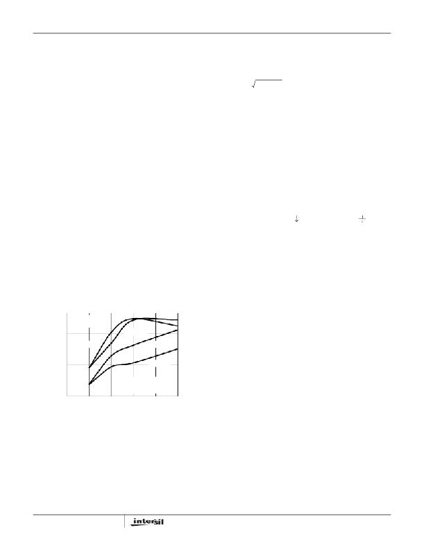
is bigger, which generates more RMS current loss. Figure 11
shows the efficiency of the demo board under different
inductance for a specific series of inductor. For optimal
efficiency in an application, it is a good exercise to check
several adjacent inductance values of your preferred series
of inductors.
For the same inductance, higher overall efficiency can be
obtained by using lower DCR inductor.
EFFICIENCY vs I O
4 LEDs can be placed in series.
However, placing LEDs into series/parallel connection can
give higher efficiency as shown in the efficiency curves. One
of the ways to ensure the brightness uniformity is to pre-
screen the LEDs.
PCB Layout Considerations
The layout is very important for the converter to function
properly. Power Ground ( ) and Signal Ground ( ) should
be separated to ensure the high pulse current in the power
ground does not interference with the sensitive signals
connected to Signal Ground. Both grounds should only be
connected at one point right at the chip. The heavy current
paths (V IN -L-L X pin-PGND, and V IN -L-D-C 2 -PGND) should
be as short as possible.
The trace connected to the CS pin is most important. The
current sense resister R 1 should be very close to the pin
When the trace is long, use a small filter capacitor close to
the CS pin.
85
83
V IN = 3.3V FOR
DIFFERENT L
L = 22μH
The heat of the IC is mainly dissipated through the PGND
pin. Maximizing the copper area around the plane is
preferable. In addition, a solid ground plane is always helpful
L = 33μH
L = 15μH
for the EMI performance.
81
79
77
L = 10μH
L = Coilcraft
LPO1704 SERIES
1mm HEIGHT
The demo board is a good example of layout based on the
principle. Please refer to the EL7513 Application Brief for the
layout.
5
10
15
20
25
30
I O (mA)
FIGURE 21. EFFICIENCY OF DIFFERENT INDUCTANCE
(4 LEDs IN A SERIES)
10
FN7112.5
December 22, 2008
发布紧急采购,3分钟左右您将得到回复。
相关PDF资料
EL7630ICZ-T7A
IC LED DRVR WHITE BCKLGT SC-70-6
EPG7236
PANEL STEEL 70.2 X 34.2"
ER2-4M-90
EMULATOR EPROM ECONOROM II 4MEG
ER3-8M
EMULATOR EPROM ECONOROM III 8MEG
ESF2424
FRAME SWING ECLIPSE 19.25X19"
ESF3024
FRAME SWING ECLIPSE 24.5X19"
ESF3624
FRAME SWING ECLIPSE 29.75X19"
ESP1212
PANEL STEEL SWING 12X12" WHT
相关代理商/技术参数
EL7515
制造商:INTERSIL 制造商全称:Intersil Corporation 功能描述:High Frequency PWM Step-Up Regulator
EL7515_07
制造商:INTERSIL 制造商全称:Intersil Corporation 功能描述:High Frequency PWM Step-Up Regulator
EL7515IY
功能描述:IC REG BOOST ADJ 0.6A 10MSOP RoHS:否 类别:集成电路 (IC) >> PMIC - 稳压器 - DC DC 开关稳压器 系列:- 产品培训模块:Lead (SnPb) Finish for COTS
Obsolescence Mitigation Program 标准包装:1 系列:- 类型:降压(降压) 输出类型:固定 输出数:1 输出电压:3.3V 输入电压:4.5 V ~ 24 V PWM 型:- 频率 - 开关:- 电流 - 输出:125mA 同步整流器:无 工作温度:-40°C ~ 85°C 安装类型:表面贴装 封装/外壳:SOT-23-6 包装:Digi-Reel® 供应商设备封装:SOT-6 其它名称:MAX1836EUT33#TG16DKR
EL7515IY-T13
功能描述:IC REG BOOST ADJ 0.6A 10MSOP RoHS:否 类别:集成电路 (IC) >> PMIC - 稳压器 - DC DC 开关稳压器 系列:- 产品培训模块:Lead (SnPb) Finish for COTS
Obsolescence Mitigation Program 标准包装:1 系列:- 类型:降压(降压) 输出类型:固定 输出数:1 输出电压:3.3V 输入电压:4.5 V ~ 24 V PWM 型:- 频率 - 开关:- 电流 - 输出:125mA 同步整流器:无 工作温度:-40°C ~ 85°C 安装类型:表面贴装 封装/外壳:SOT-23-6 包装:Digi-Reel® 供应商设备封装:SOT-6 其它名称:MAX1836EUT33#TG16DKR
EL7515IY-T7
功能描述:IC REG BOOST ADJ 0.6A 10MSOP RoHS:否 类别:集成电路 (IC) >> PMIC - 稳压器 - DC DC 开关稳压器 系列:- 产品培训模块:Lead (SnPb) Finish for COTS
Obsolescence Mitigation Program 标准包装:2,500 系列:- 类型:降压(降压) 输出类型:两者兼有 输出数:1 输出电压:5V,1 V ~ 10 V 输入电压:3.5 V ~ 28 V PWM 型:电流模式 频率 - 开关:220kHz ~ 1MHz 电流 - 输出:600mA 同步整流器:无 工作温度:-40°C ~ 125°C 安装类型:表面贴装 封装/外壳:16-SSOP(0.154",3.90mm 宽) 包装:带卷 (TR) 供应商设备封装:16-QSOP
EL7515IYZ
功能描述:直流/直流开关调节器 EL7515IYZ HI EFFOO STG RoHS:否 制造商:International Rectifier 最大输入电压:21 V 开关频率:1.5 MHz 输出电压:0.5 V to 0.86 V 输出电流:4 A 输出端数量: 最大工作温度: 安装风格:SMD/SMT 封装 / 箱体:PQFN 4 x 5
EL7515IYZS2695
制造商:Intersil Corporation 功能描述:EL7515IYZ - FOR TRACKING PURPOSES ONLY, USES PL CODE D3W - Rail/Tube
EL7515IYZT13
制造商:INTERSIL 制造商全称:Intersil Corporation 功能描述:High Frequency PWM Step-Up Regulator
